DELTA, SUPERLATTICE DOPING AND ALD SERVICES
INTRODUCTION
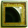
FastVision is capable of processing sensor wafers on a contract basis to produce backside illuminated wafers sensitive in the UV and soft X-Ray region with an array of anti-reflective coatings based on licensed patented, (US 8,395,243 and US 8,680,637), technology from Jet Propulsion Laboratory (JPL).
Back-illumination enables high quantum efficiency and 100% fill factor in CMOS imaging detectors at visible wavelengths. Ultraviolet (and electron) detection is significantly more challenging for several reasons. First, strong absorption in the ultraviolet makes the sensors with detector quantum efficiency exceptionally sensitive to the Si-SiO2 interface trap density. Second, deep ultraviolet photons create interface traps that rapidly degrade detectors, causing loss of efficiency and unstable response. Third, CMOS imaging detectors cannot withstand high temperature processing, which makes it impossible to repair detectors once they have been damaged by deep ultraviolet (DUV) radiation.
Conventional methods of surface passivation require low defect densities at the interface. Deep ultraviolet radiation damages the interface, and over time, DUV exposure creates a high density of interface traps that significantly degrades detector performance. Thus DUV-damaged detectors are subject to low and unstable quantum efficiency, high dark current, and hysteresis. Hardening of the oxide can slow DUV-induced degradation, but DUV stability remains a major problem in silicon detectors passivated by conventional methods such as ion implantation, diffusion, or chemisorption charging.
Surface passivation methods developed by the Jet Propulsion Laboratory are unique in their exceptional tolerance to DUV damage. Stable, high quantum efficiency is observed in these detectors even after extended exposure to high intensity, pulsed excimer laser radiation. JPL's surface passivation technology is based on low temperature silicon molecular beam epitaxy, which is used to create a surface dopant density that is one to two orders of magnitude higher than the silicon solid solubility limit. At these dopant densities, MBE-grown surface passivation layers need only extend 2 or 3 nm into the surface to completely isolate the detector from the effects of surface traps. On this length scale, photogenerated electrons are quantum-mechanically excluded from the surface on picosecond timescales, virtually eliminating losses due to recombination. Finally, immunity from interface defects creates enormous flexibility in the development of antireflection coatings.
2D LAYERED GROWTH (SUPERLATTICE) VERSUS 3D GROWTH
The structural distinction between 2D versus 3D doping is that in standard MBE growth, doped silicon is grown using 3D doping methods, which involves co-deposition of silicon and dopants (boron in this case) on the surface. In 2D doping, silicon and boron are not co-deposited, but are instead deposited alternately (first silicon, then boron, then silicon, then boron, etc., with the first and last layers always comprising silicon). The growth mechanism for 2D doping is fundamentally different from 3D doping, with the net result that you can incorporate 1 to 2 orders of magnitude higher dopant concentrations using 2D doping methods.
In 3D doping, dopants are incorporated randomly into the crystal--the dopant concentration is nominally controlled by adjusting the relative fluxes of silicon and boron to achieve the right ratio; however, at high dopant concentrations, thermodynamics can intervene, because above a certain concentration it is observed that not all deposited dopants are actually incorporated into electrically active sites in the growing crystal. In 2D doping, dopants are confined to a finite number of two-dimensional planes within the three-dimensional crystal lattice. The 2D doping technique takes advantage of thermodynamics, in that within each layer, the dopant atoms form a self-organized surface phase; this ordering within the crystal is stabilized by growing silicon on top of the 2D dopant layer. There is a fundamental difference between the structures formed by 3D doping as compared to 2D doping. In 3D doping, dopants are distributed randomly. In 2D doping, dopants are ordered within the crystal lattice. Because of the ordering, it is possible to make better detectors. Delta-doping (single-layer 2D doping) is better than 3D doping because it allows one to grow thinner passivation layer and at the same time achieve higher incorporation of dopants (in this case, the 3D- doped layer had 1x10^14 dopants/cm^2 in a 5nm layer, while delta-doping achieved 2x10^14 dopants/cm^-2 in 2.5nm---in other words, twice the doping, in half the thickness).
Multilayer (Superlattice) doping was motivated by applications that required the detector to be hit by powerful lasers in the deep ultraviolet, which are known to damage detectors. The surface in terms of quantum mechanics gives a very different answer, and the performance did not have to suffer from the thicker MBE layers that would be required for multilayer 2D doping. When multilayer (superlattice) oped detectors were tested, it was found that they were significantly more robust than 3D doped detectors (as expected, because of the increased dopant density), but we also proved the unexpected result that the quantum efficiency can be just as high with multilayer doping as with delta-doping. In other words, 2D doping achieves performance advantages (exceptional stability and quantum efficiency even when exposed to DUV lasers) that cannot be achieved using 3D doping methods These performance advantages are tied to structure---judged by detector performance, the structure formed by multilayer 2D doping is superior to the structures that are possible with 3D doping.
WAFER OR SENSOR PROCESSING
In order to produce delta or superlattice doped sensor wafer the following steps are used:
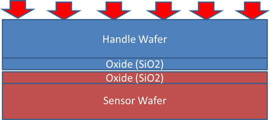
- Attach a handle wafer
- Back side thinning (BST)
- Super-lattice (Delta)-Doping (SLD)
- Anti-reflective coating (AR)
- Optional opening the pads and streets
Delta doping is a process by which a large surface potential is created to direct photoelectrons generated at the surface toward the photo diodes of an imaging array. The penetration depth of (UV) photons into silicon is tens of nanometers. Photoelectrons generated by (UV) photons recombine without propagating to the photo diodes in the absence of passivatio because they are trapped near the surface. In addition the photo diodes experience a lateral capture effects in BSI applications, effectively increasing the fill factor to 100% in BSI applications.
ATTACHING A HANDLE WAFER
The handle wafer which is a approximately 700 um silicon wafer is attached to the front side of the sensor wafer by a proprietary oxide to oxide bonding process. This process varies according to the thickness of native oxide on front surface of the sensor wafer, the flatness of sensor wafer and is a low temperature process consistent with most CMOS, CCD and APD processes.
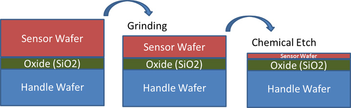
BACK SIDE THINNING (BST)
BST is achieve by first mechanically grinding the back side of the sensor wafer to leave a thickness close to the desired thickness which is determined by the desired wavelength response and the spi thickness of the sensor wafer Then chemical etching is applied to allow thinning into the top layers of the epi and achieve the desired smothness and flatness over the entire wafer which is usuallly in the order of 2 um.
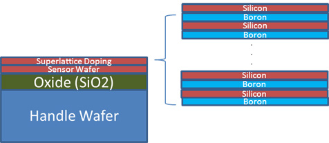
DELTA AND SUPERLATTICE DOPING
Delta or superlattice doping is the deposition using molecular beam epitaxy (MBE) to deposit one to six Boron and Silicon layers. This is a multistep process where the number of layers is a trade off between the Modulation transfer function (MTF) and durability at the target frequency and power resiliance. This uses a thinned wafer with deposition on the epi layer of the sensor side and requires temperatures in the 400 to 450 degrees Celsius for a brief period.
ANTIREFLECTIVE (AR) COATINGS OFTEN USING ALD
Antireflective (AR) coatings are applied to the back of the sensor to reduce the loss of photons due to reflection of the bare silicon surface. Over one half of the photons are lost to reflection in the absence of AR coatings AR coatings can be designed for specific wave lengths for example an AR coating for 263 nm can improve transmission to above 90%. AR coatings for 193 nm have approached over 80% transmission depending on the energies involved. Antireflective coatings Can be directly deposited or formed, e.g. native oxide or deposited in a more controlled fashion using Atomic layer Deposition (ALD) which is frequently used. Examples of mono-layer deep ultra-violet (DUV) and extreme ultra-violate (EUV) coatings which can be deposited by ALD are Silicon Dioxide, Magnesium Floride, Aluminum Oxide, and Hafnium Oxide. Also multi-layer coatings can be deposited by ALD to produce customized coating with desired operational wavelength passband /stopband, quantum efficiency (QE) and durability.

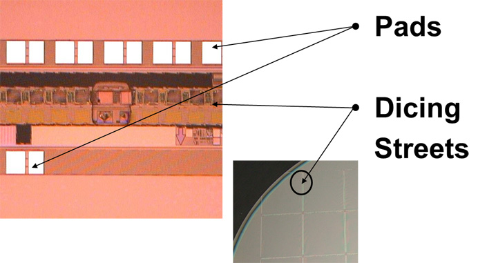
PAD AND STREET OPENING (OPTIONAL)
Optional pad and street opening of a processed wafer uses masked chemical etching and multiple masks may be needed depending on sensor architecture.
Click here to download presentation